
Leitfähige Silikonteile vereinen die Flexibilität, Temperaturbeständigkeit und Dichtungsfähigkeit von Silikonkautschuk mit einem elektrisch leitfähigen Füllstoffsystem. Sie finden breite Anwendung in elektronischen Tastaturen, Erdungskontakten, Batterieschnittstellen, EMI-Abschirmdichtungen, Sensorbaugruppen und kundenspezifischen elektrischen Steckverbindern.
Die Auswahl von leitfähigem Silikon allein auf der Grundlage eines niedrigen spezifischen Volumenwiderstands kann jedoch zu enttäuschenden Ergebnissen führen. Der Widerstand des fertigen Bauteils hängt auch von dessen Dicke, der Kontaktfläche, der Kompression, der Elektrodenoberfläche, Verunreinigungen und der langfristigen mechanischen Relaxation ab.
Um eine zuverlässige elektrische Leistung zu gewährleisten, müssen Ingenieure drei miteinander verbundene Parameter bewerten:
- Volumenwiderstand der Silikonmischung
- Kompression und Kompressionskraft
- Kontaktwiderstand des zusammengebauten Bauteils
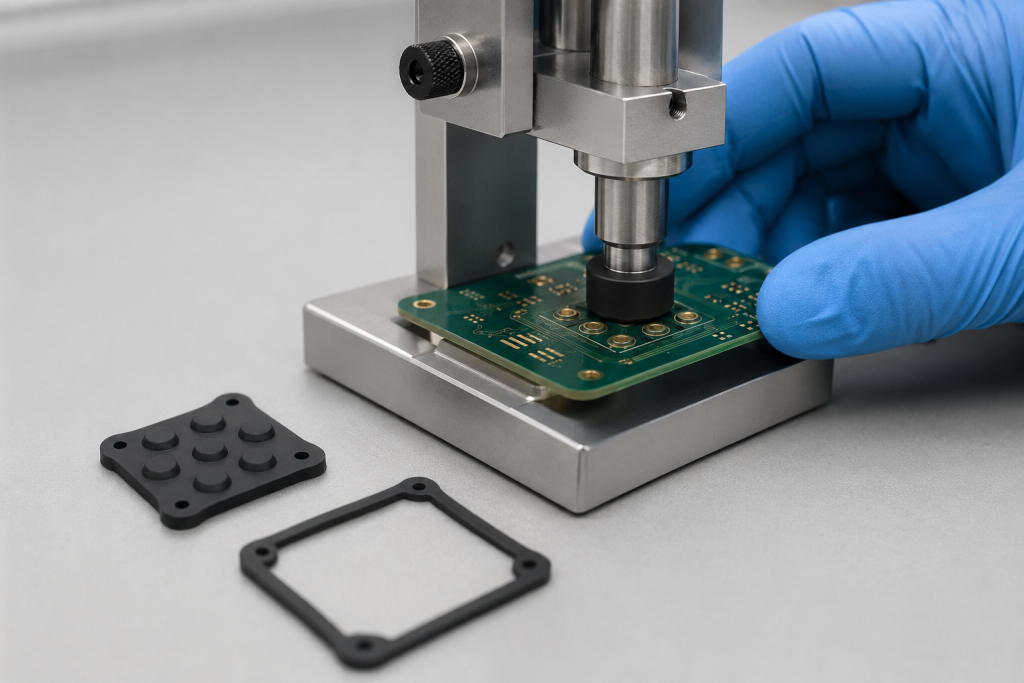
Was ist leitfähiger Silikonkautschuk?
Herkömmlicher Silikonkautschuk ist ein elektrischer Isolator. Leitfähiges Silikon wird hergestellt, indem leitfähige Partikel in die Silikonmatrix eingearbeitet werden.
Zu den gängigen leitfähigen Füllstoffen gehören:
- Ruß
- Graphit
- Nickelbeschichtetes Graphit
- Silberbeschichtetes Aluminium
- Silberbeschichtetes Kupfer
- Silberpartikel
- Sonstige metallische oder beschichtete Partikel
Shin-Etsu beschreibt elektrisch leitfähige Silikonprodukte als Silikonkautschuk, der mit Kohlenstoff und anderen leitfähigen Materialien versetzt ist. Die von dem Unternehmen veröffentlichten Produktbeispiele zeigen zudem, dass der spezifische Volumenwiderstand je nach Rezeptur erheblich variieren kann. Elektrisch leitfähige Gummiprodukte von Shin-Etsu
Der Füllstoff bildet leitfähige Bahnen durch das ausgehärtete Silikon. Sind Füllstoffkonzentration, Verteilung und Partikelkontakt ausreichend, kann Strom durch das Elastomer fließen.
Eine Erhöhung des Anteils an leitfähigen Füllstoffen kann die Leitfähigkeit verbessern, kann jedoch auch folgende Auswirkungen haben:
- Härte
- Dehnung
- Reißfestigkeit
- Druckverformungsrest
- Spritzgussfluss
- Oberflächenqualität
- Formverschleiß
- Materialkosten
Das beste Material ist daher nicht automatisch die Verbindung mit dem niedrigsten spezifischen Widerstand. Es ist vielmehr die Verbindung, die sowohl die elektrischen als auch die mechanischen Anforderungen des fertigen Produkts erfüllt.
Häufige Anwendungsbereiche
Leitfähige Silikonbauteile werden für verschiedene elektrische Funktionen eingesetzt.
Elektronische Tastaturkontakte
Eine leitfähige Silikonkapsel oder ein geformter Kontakt schließt einen Stromkreis, wenn ein Knopf gegen die Kontaktflächen der Leiterplatte gedrückt wird. Die wichtigsten Anforderungen sind in der Regel:
- Konstanter Kontaktwiderstand
- Gleichmäßige taktile Bewegung
- Geringer Rückprall
- Lange Lebensdauer
- Sauberes Ablösen von der Leiterplatte
- Widerstandsstabilität nach Alterung
Erdungskontakte
Leitfähige Silikonpolster können eine Leiterplatte, ein Gehäuse oder eine Abschirmung mit Masse verbinden und dabei Maßabweichungen und Vibrationen ausgleichen.
EMI-Abschirmdichtungen
Leitfähige Silikondichtungen gewährleisten den elektrischen Durchgang zwischen den Gehäuseoberflächen und dienen gleichzeitig als Umgebungsabdichtung.
Parker Chomerics bietet leitfähige Silikon- und Fluorsilikon-Dichtungen mit Füllstoffen wie Nickel-Aluminium, Nickel-Graphit, Silber-Aluminium und Silber-Kupfer an. Das Unternehmen weist darauf hin, dass leitfähige Elastomer-Dichtungen sowohl eine EMI-Abschirmung als auch eine Umgebungsabdichtung gewährleisten können. Leitfähige Elastomer-Dichtungen von Parker Chomerics
Flexible elektrische Schnittstellen
Maßgefertigte leitfähige Silikonkomponenten können einen nachgiebigen Kontakt gewährleisten, wo starre Metallfedern nur schwer unterzubringen oder anfällig für Vibrationen wären.
Ableitung statischer Elektrizität
Manche Werkstoffformulierungen sind darauf ausgelegt, statische Elektrizität abzuleiten, anstatt Betriebsstrom zu leiten. Die Anforderungen an Leitfähigkeit, statische Ableitung und Antistatik sollten nicht als austauschbar betrachtet werden.
Volumenwiderstand
Der spezifische Volumenwiderstand beschreibt, wie stark ein Material dem Durchfluss von elektrischem Strom durch sein Volumen widersteht. Ein niedrigerer spezifischer Volumenwiderstand weist auf eine höhere Leitfähigkeit hin.
Es wird normalerweise ausgedrückt als:
- Ω·cm
- Ω·m
Die Beziehung lautet:
ρ = R × A ÷ L
Wo:
- ρ ist der spezifische Volumenwiderstand
- R ist der gemessene Widerstand
- A ist die Kontaktfläche der Elektrode
- L ist die Probenstärke oder die Länge des Strompfads
Der ungefähre Widerstand durch ein Bauteil lässt sich daher wie folgt abschätzen:
R = ρ × L ÷ A
Diese Gleichung verdeutlicht, warum zwei aus demselben leitfähigen Silikon geformte Bauteile unterschiedliche Widerstandswerte aufweisen können. Ein dicker, schmaler Strompfad führt in der Regel zu einem höheren Volumenwiderstand als ein dünnes Bauteil mit großer Kontaktfläche.
Der spezifische Volumenwiderstand ist eine Materialeigenschaft – unter definierten Bedingungen
Die Norm ASTM D991 regelt die Bestimmung des spezifischen Volumenwiderstands von elektrisch leitfähigen und antistatischen Gummiprodukten. Das Verfahren geht davon aus, dass die Oberflächenleitfähigkeit im Vergleich zur Leitfähigkeit durch die Probe vernachlässigbar ist. ASTM D991-89(2026)
Ein veröffentlichter Widerstandswert sollte stets in Verbindung mit folgenden Angaben überprüft werden:
- Prüfverfahren
- Abmessungen der Probe
- Elektrodenkonfiguration
- Angewandte Spannung oder Stromstärke
- Umgebungsbedingungen
- Heilungsbedingungen
- Bedingungen nach der Aushärtung
- Temperatur
- Messrichtung
- Ausgeübter Druck
Die in den technischen Datenblättern der Lieferanten angegebenen Werte sind zwar für die Materialauswahl hilfreich, garantieren jedoch nicht die Beständigkeit eines fertigen Formteils.
Die Umrechnung der Einheiten muss überprüft werden
Der spezifische Volumenwiderstand wird üblicherweise sowohl in Ω·m als auch in Ω·cm angegeben.
1 Ω·m = 100 Ω·cm
Der Vergleich zweier Datenblätter ohne Umrechnung der Einheiten kann zu einem 100-fachen Interpretationsfehler führen.
Wie sich Kompression auf die Leitfähigkeit auswirkt
Durch die Kompression verändern sich sowohl das interne Leitungsnetzwerk als auch die Grenzfläche zwischen dem Silikon und der Gegenelektrode.
Der Kompressionsprozentsatz lässt sich wie folgt berechnen:
Kompression (%) = (ursprüngliche Dicke − komprimierte Dicke) ÷ ursprüngliche Dicke × 100
Wird beispielsweise ein 2,0 mm dickes leitfähiges Pad auf 1,6 mm zusammengedrückt, beträgt die nominelle Kompression 20%.
Diese Zahl allein reicht nicht aus. Ingenieure müssen außerdem die Druckkraft, die Kontaktfläche und den Toleranzbereich kennen.
Unzureichende Kompression
Eine zu geringe Kompression kann folgende Folgen haben:
- Unvollständiger Kontakt mit der Elektrode
- Hoher oder instabiler Widerstand
- Vibrationsempfindlichkeit
- Zeitweise unterbrochene elektrische Verbindung
- Mangelhafte EMI-Abschirmung
- Undichtigkeit an einer Umweltschutzdichtung
- Erhöhte Empfindlichkeit gegenüber Oberflächenverunreinigungen
Kontrollierte Kompression
Innerhalb eines geeigneten Arbeitsbereichs vergrößert die Kompression in der Regel die tatsächliche Kontaktfläche und stabilisiert die leitenden Pfade zwischen dem Elastomer und den Gegenflächen.
Der richtige Kompressionsbereich muss anhand folgender Faktoren ermittelt werden:
- Materialhärte
- Teileprofil
- Wandstärke
- Kontaktbereich
- Druck-Durchbiegungs-Kurve
- Erforderliche Schließkraft
- Steifigkeit des Gehäuses
- Langzeit-Druckverformungsrest
Übermäßige Kompression
Eine stärkere Kompression ist nicht immer besser. Eine übermäßige Kompression kann folgende Auswirkungen haben:
- Zu hohe Montagekraft
- Biegen von Leiterplatten
- Verzerrungen auf dem Wohnungsmarkt
- Silikonaustritt aus der Nut
- Dauerverformung
- Rissbildung an dünnen Stellen
- Beschleunigte Spannungsrelaxation
- Schäden an benachbarten Bauteilen
- Schwierige Demontage
- Verkürzte Lebensdauer
Verwenden Sie, soweit möglich, mechanische Kompressionsanschläge. Diese verhindern, dass Schrauben oder Gehäusetoleranzen das leitfähige Silikon übermäßig komprimieren.
Druckkraft im Vergleich zum Kompressionsprozentsatz
Zwei leitfähige Teile, die um denselben Prozentsatz zusammengedrückt werden, können sehr unterschiedliche Kräfte erzeugen.
Die Druckkraft hängt ab von:
- Silikonhärte
- Art und Konzentration des Füllstoffs
- Querschnittsprofil
- Teilstärke
- Kontaktbereich
- Dehnungsgeschwindigkeit
- Temperatur
- Geschichte der Alterung
Eine weiche, hohle oder P-förmige Dichtung erfordert unter Umständen eine deutlich geringere Anpresskraft als ein massiver rechteckiger Streifen. Parker beispielsweise beschreibt seine leitfähige Dichtung CHO-SEAL 1299 mit niedriger Härte als Option mit geringerer Anpresskraft für EMI-Abschirmungsanwendungen. Parker Chomerics CHO-SEAL 1299
Wenn der leitfähige Teil mit einer Leiterplatte oder einem dünnen Kunststoffgehäuse in Kontakt kommt, berechnen Sie die maximale Montagebelastung, bevor Sie das Dichtungsprofil endgültig festlegen.
Was ist Kontaktwiderstand?
Der Kontaktwiderstand ist der Widerstand, der an der Stelle gemessen wird, an der das leitfähige Silikon auf eine Elektrode, eine Leiterplattenkontaktfläche, ein Metallgehäuse oder eine andere leitfähige Oberfläche trifft.
Es ist nicht mit dem Volumenwiderstand identisch.
Der gemessene Widerstand eines montierten leitfähigen Silikonkontakts kann Folgendes umfassen:
- Volumenwiderstand durch das Silikon
- Widerstand an der ersten Grenzfläche zwischen Silikon und Elektrode
- Widerstand an der zweiten Schnittstelle
- Oberflächenfilmwiderstand
- Widerstand gegen Verengung an einzelnen Kontaktpunkten
- Leuchten- und Leitungswiderstand
- Anschlusswiderstand im Messsystem
In der Norm ASTM B539 wird erläutert, dass der Kontaktwiderstand den Verengungswiderstand und den Schichtwiderstand umfasst. Außerdem wird darauf hingewiesen, dass tatsächliche Kontaktflächen nicht aus der gesamten scheinbaren Oberfläche bestehen, sondern aus vielen kleinen Kontaktpunkten. ASTM B539-20(2026)
Obwohl sich die Norm ASTM B539 in erster Linie auf statische elektrische Verbindungen bezieht, ist dieses Prinzip bei der Entwicklung eines Prüfverfahrens auf Bauteilebene für leitfähige Silikonbaugruppen von großer Bedeutung.
Warum ein niedriger Volumenwiderstand keinen niedrigen Kontaktwiderstand garantiert
Ein Verbundwerkstoff kann zwar eine hervorragende Volumeleitfähigkeit aufweisen, während die fertige Baugruppe dennoch einen zu hohen Widerstand aufweist.
Mögliche Gründe sind unter anderem:
- Unzureichende Kompression
- Kleine wirksame Kontaktfläche
- Oxid auf der Metalloberfläche
- PCB-Belastung
- Mold-release residue
- Silicone oil or processing residue
- Dust or fingerprints
- Rough or uneven mating surfaces
- Incorrect electrode plating
- Part warpage
- Uneven pressure distribution
- Loss of force after aging
For this reason, the product specification should normally contain both:
- A material-level volume-resistivity requirement
- A component-level contact-resistance requirement under defined assembly conditions
Contact Surface Design
Provide Adequate Contact Area
A larger contact area can reduce current density and improve resistance stability. However, the useful electrical contact area may be much smaller than the visible geometric area if pressure is uneven.
Control Surface Flatness
Warped housings or PCB assemblies can create local gaps. The tolerance stack should include:
- Conductive silicone thickness
- Rillentiefe
- Ebenheit des Gehäuses
- PCB flatness
- Insert height
- Fastener location
- Compression-stop height
Review the Electrode Material and Plating
Bare copper, nickel, tin, gold, aluminum and conductive coatings have different oxidation and corrosion behavior.
Gold-plated PCB contacts are often used where stable, low-level switching performance is important, while enclosure grounding applications may use different metal finishes depending on cost and environment.
Material pairs should also be evaluated for galvanic compatibility, especially in humid or salt-containing environments.
Avoid Contaminating the Contact Zone
Mold-release agents, lubricants, adhesives and cleaning chemicals can increase resistance. If these substances are required elsewhere in the assembly, keep them away from the electrical contact area and verify compatibility through testing.
Use Localized Contact Features Carefully
Small domes, ribs or raised pads can concentrate force and help break through light surface films. However, excessive local stress may cause wear, permanent deformation or damage to PCB coatings.
Conductive Filler Selection
| Filler system | General characteristics | Typical considerations |
|---|---|---|
| Carbon-based | Cost-effective, suitable for switches and static control | Higher resistance than many metal-filled systems |
| Nickel-graphite | Common for EMI shielding and grounding | Balance of shielding performance and cost |
| Silver-aluminum | High conductivity with suitability for aluminum enclosures | Höhere Materialkosten |
| Silver-copper | Very high conductivity | Corrosion and galvanic compatibility must be evaluated |
| Pure silver | Excellent conductivity | Highest cost and not necessary for every application |
| Conductive-coated particles | Performance can be adjusted through particle core and coating | Supplier-specific conductivity and aging behavior |
Filler descriptions are general. Actual performance depends on particle morphology, loading, dispersion, silicone formulation and curing process.
Do not approve a filler system based only on its chemical name. Test the production compound in the actual component geometry.
Material Hardness and Compression Set
Conductive silicone hardness affects both assembly force and contact stability.
Softer Materials
Zu den potenziellen Vorteilen zählen:
- Lower closing force
- Bessere Anpassung an unebene Oberflächen
- Improved contact at low compression
- Reduced stress on PCBs and housings
Zu den möglichen Nachteilen zählen:
- Greater extrusion risk
- More difficult dimensional control
- Increased handling deformation
- Potentially lower tear strength
Harder Materials
Zu den potenziellen Vorteilen zählen:
- Bessere Formbeständigkeit
- Higher localized contact pressure
- Improved handling
- Reduced extrusion in some designs
Zu den möglichen Nachteilen zählen:
- Higher assembly force
- Greater risk of housing or PCB deformation
- Reduced conformity to irregular surfaces
Compression set indicates how much deformation remains after the material has been compressed for a specified time and temperature. Lower compression set is generally desirable for maintaining contact force, but the published test condition must match the application closely enough to be meaningful.
Designing Different Conductive Silicone Components
Conductive Keypad Pills
A conductive pill is normally molded or bonded to the underside of a silicone button.
Zu den wichtigen Auslegungsparametern gehören:
- Pill diameter
- Pill thickness
- Ebenheit
- Alignment with PCB traces
- Button travel
- Actuation force
- Overtravel
- Kontaktwiderstand
- Release characteristics
- Cycle-life requirement
The contact-resistance specification should identify the applied button force or travel position. A resistance limit without an actuation condition is incomplete.
Conductive Silicone Gaskets
For enclosure gaskets, evaluate electrical continuity and environmental sealing simultaneously.
Rezension:
- Gasket profile
- Nutabmessungen
- Compression range
- Closure force
- Befestigungsabstand
- Enclosure stiffness
- Oberflächenbeschichtung
- EMI frequency range
- Water or dust sealing requirement
- Environmental aging
A gasket can maintain a water seal but still lose acceptable electrical continuity, or maintain conductivity while failing the environmental seal. Both functions require separate validation.
Conductive Contact Pads
A conductive pad placed between a PCB and housing should be thick enough to accommodate tolerances without generating excessive force.
Large unsupported pads may buckle, slide or compress unevenly. Alignment ribs, pockets or adhesive-backed carriers can improve assembly repeatability, provided the adhesive does not enter the conductive path.
Multi-Material Silicone Parts
Conductive and nonconductive silicone can be combined within one component to create isolated conductive zones.
Critical issues include:
- Material bonding
- Positional accuracy
- Conductive-path separation
- Flash between zones
- Cure compatibility
- Schrumpfungsunterschied
- Tooling complexity
- Electrical leakage between adjacent contacts
Each conductive zone should be tested independently.
Measuring Contact Resistance
A four-wire Kelvin method is normally preferred for low-resistance measurements because it reduces the influence of test-lead resistance.
The test fixture should define:
- Electrode material
- Electrode plating
- Electrode dimensions
- Oberflächenbeschaffenheit
- Reinigungsverfahren
- Kompressionsprozentsatz
- Applied force
- Compression speed
- Dwell time before measurement
- Test current
- Open-circuit voltage
- Temperatur und Luftfeuchtigkeit
- Number and location of measurements
IEC 60512-2-1 defines a millivolt-level method for measuring contact resistance across mated contacts or a contact with a measuring gauge. IEC 60512-2-1:2002
IEC 60512-2-2 provides a specified-test-current method. IEC 60512-2-2:2003
The most appropriate method depends on whether the conductive silicone is used for low-level signals, switching, grounding, EMI control or current transmission.
Test Resistance Across the Compression Range
Do not test only at nominal compression. Measure at:
- Minimum compression
- Nominal compression
- Maximum compression
This reveals whether tolerance variation can produce an open circuit, excessive resistance or damaging assembly force.
A useful validation graph plots:
- Contact resistance versus compression
- Compression force versus compression
The acceptable production window is the region where both electrical resistance and mechanical force meet the design requirements.
Environmental and Life Testing
Conductive silicone performance should be checked before and after relevant environmental exposure.
Possible tests include:
- Hochtemperaturalterung
- Einwirkung niedriger Temperaturen
- Temperature cycling
- Damp heat or humidity
- Salt mist for exposed metal interfaces
- Exposition gegenüber Chemikalien
- UV and weathering
- Vibration
- Mechanischer Stoß
- Repeated compression
- Keypad actuation cycling
- Long-term static compression
- Storage aging
Record both the initial resistance and the change after exposure. A component that initially passes but shows unstable resistance after aging may not be suitable for production.
Current-Carrying Limitations
Conductive silicone should not automatically be treated as a replacement for a copper conductor.
The acceptable current depends on:
- Spezifischer Volumenwiderstand
- Current-path length
- Kontaktbereich
- Kontaktwiderstand
- Duty cycle
- Heat dissipation
- Ambient temperature
- Allowable temperature rise
- Material aging
- Failure consequences
High resistance can generate localized heat according to:
Power = Current² × Resistance
Applications involving meaningful current should include temperature-rise testing under worst-case compression, voltage, current and ambient-temperature conditions.
Überlegungen zur Fertigung
Conductive silicone parts may be manufactured by:
- Formpressen
- Transferformverfahren
- Spritzguss
- Liquid silicone rubber molding
- Extrusion and cutting
- Die cutting from conductive silicone sheet
- Co-molding with nonconductive silicone
- Overmolding onto metal or plastic inserts
High filler loading can affect flow and mold filling. Thin ribs, narrow channels and small conductive zones may require different tooling and process conditions from conventional silicone parts.
Production controls may include:
- Rückverfolgbarkeit von Materialchargen
- Kontrolliertes Mischen
- Cure-temperature monitoring
- Cure-time verification
- Post-cure control
- Part-weight monitoring
- Maßprüfung
- Resistance testing
- Visual inspection for contamination and flash
Common Problems and Corrective Directions
| Problem | Possible causes | Korrekturrichtung |
| Resistance too high | Incorrect material, long current path, small area | Review resistivity, thickness and contact area |
| Resistance changes with movement | Insufficient compression or uneven pressure | Improve support and compression control |
| High initial resistance | Surface contamination or oxide | Review cleaning and electrode finish |
| Resistance increases after aging | Compression set, corrosion or material degradation | Test alternative material and interface finishes |
| PCB bends during assembly | Excessive compression force | Use softer material, revised profile or compression stops |
| Conductive part extrudes from groove | Excessive compression or poor retention | Adjust groove, tolerance and material hardness |
| Inconsistent keypad response | Pill misalignment or variable button travel | Improve tooling, assembly location and travel control |
| Gasket passes sealing but fails grounding | Environmental seal and electrical path are not equivalent | Validate both functions independently |
| Adjacent contacts short circuit | Conductive flash or inadequate spacing | Improve shut-offs, inspection and contact separation |
Prototype and Validation Plan
A practical development sequence includes:
- Select candidate compounds based on resistivity, hardness and environmental requirements.
- Mold simple material specimens and production-representative parts.
- Measure volume resistivity using a defined method.
- Generate compression-force curves.
- Measure contact resistance at minimum, nominal and maximum compression.
- Test the intended electrode material and plating.
- Complete temperature, humidity and cycling tests.
- Evaluate dimensional and electrical variation by cavity.
- Run pilot production using the intended manufacturing process.
- Establish production inspection limits and sampling frequency.
Do not finalize the production specification using only prototype parts manually selected for good performance.
Checkliste für Angebotsanfragen
Provide the following information when requesting a quotation:
- 2D-Zeichnung und 3D-Modell
- Part application
- Required electrical function
- Target volume resistivity
- Maximum assembled contact resistance
- Test current and voltage
- Required current-carrying capacity
- Nominal, minimum and maximum compression
- Maximum allowable compression force
- Electrode material and plating
- Betriebstemperatur
- Humidity and chemical exposure
- EMI shielding requirement
- Environmental sealing requirement
- Hardness range
- Color limitations
- Flame-retardant requirements
- Jährliches Produktionsvolumen
- Erforderliche Lebensdauer
- Gesetzliche Anforderungen
- Anforderungen an die Kontrolle und Rückverfolgbarkeit
If the electrical specification is not yet established, provide the complete assembly geometry and functional requirement. The molding supplier can then help develop suitable test conditions and material options.
Häufig gestellte Fragen
What volume resistivity should conductive silicone have?
There is no universal target. Static-dissipative parts, keypad contacts, EMI gaskets and current-carrying contacts require different conductivity levels. Define the maximum finished-part resistance and operating conditions before selecting the material.
Does compressing conductive silicone reduce resistance?
Controlled compression usually improves contact stability and can lower the measured assembly resistance. However, excessive compression can damage the part, overload the housing and reduce long-term reliability.
Is volume resistivity the same as contact resistance?
No. Volume resistivity describes the bulk material, while contact resistance includes the interfaces between the silicone and mating electrodes.
Why does a sample pass but the assembled product fail?
The assembly may have insufficient compression, surface contamination, uneven loading, electrode oxidation or an unfavorable geometry even when the material itself meets its resistivity specification.
Can conductive silicone carry electrical current?
It can carry current within application-specific limits, but it generally has much higher resistance than metal conductors. Temperature-rise and aging tests are required for current-carrying applications.
Can conductive and insulating silicone be molded together?
Yes. Multi-material molding can create isolated conductive contacts within an insulating silicone body. Bonding, positional tolerance, material compatibility and conductive flash must be carefully controlled.
How should conductive silicone contact resistance be measured?
Use a defined fixture—preferably with a four-wire measurement arrangement—and specify electrode material, surface finish, compression, force, dwell time, voltage, current and environmental conditions.
Can conductive silicone provide both EMI shielding and waterproof sealing?
Yes, some conductive elastomer gaskets are designed for both functions. Electrical continuity and environmental sealing must still be validated separately.
Fazit
A reliable conductive silicone component cannot be specified with one resistivity number alone. Volume resistivity determines the material’s bulk conductivity, while component geometry, compression and electrode conditions determine the actual assembled contact resistance.
The best development process combines material testing, compression-force analysis, part-level resistance measurement and environmental validation. Send your drawing, assembly structure, electrical requirements, compression range and operating environment for a conductive silicone DFM and material-selection review.
 English
  Japanese
  Korean
  German
  French
  Italian
  Spanish
  Dutch
Dutch  Chinese
  Portuguese
  Polish
  Czech
Czech  Hungarian
  Swedish
  Finnish
  Vietnamese
  Thai
Thai  Turkish
  Arabic
  Russian