
Conductive silicone parts combine the flexibility, temperature resistance and sealing capability of silicone rubber with an electrically conductive filler system. They are widely used in electronic keypads, grounding contacts, battery interfaces, EMI shielding gaskets, sensor assemblies and custom electrical connectors.
However, selecting conductive silicone based only on a low volume-resistivity value can produce disappointing results. The finished component’s resistance also depends on its thickness, contact area, compression, electrode surface, contamination and long-term mechanical relaxation.
For reliable electrical performance, engineers must evaluate three connected parameters:
- Volume resistivity of the silicone compound
- Compression and compression force
- Contact resistance of the assembled component
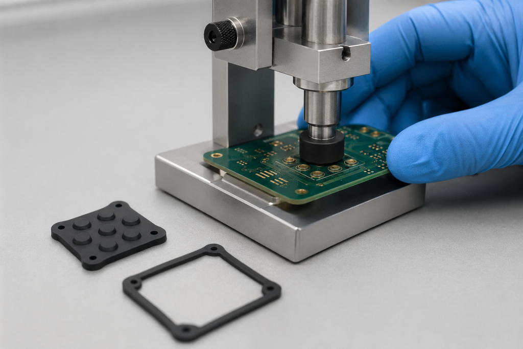
What Is Conductive Silicone Rubber?
Standard silicone rubber is an electrical insulator. Conductive silicone is produced by incorporating conductive particles into the silicone matrix.
Common conductive fillers include:
- 炭黑
- Graphite
- Nickel-coated graphite
- Silver-coated aluminum
- Silver-coated copper
- Silver particles
- Other metallic or coated particles
Shin-Etsu describes electrically conductive silicone products as silicone rubber compounded with carbon and other conductive materials. Its published product examples also demonstrate that volume resistivity can vary substantially between formulations. Shin-Etsu electrically conductive rubber products
The filler forms conductive paths through the cured silicone. When filler concentration, distribution and particle contact are sufficient, electricity can pass through the elastomer.
Increasing conductive filler loading can improve conductivity, but it may also affect:
- 硬度
- 伸長率
- 抗撕裂強度
- 壓縮永久變形
- Molding flow
- 表面品質
- 模具磨損
- Material cost
The best material is therefore not automatically the compound with the lowest resistivity. It is the compound that meets both the electrical and mechanical requirements of the assembled product.
Common Applications
Conductive silicone components are used for several different electrical functions.
Electronic Keypad Contacts
A conductive silicone pill or molded contact closes a circuit when a button is pressed against PCB contact pads. The important requirements are usually:
- Stable contact resistance
- Consistent tactile movement
- Low bounce
- Long cycle life
- Clean release from the PCB
- Resistance stability after aging
Grounding Contacts
Conductive silicone pads can connect a PCB, housing or shield to ground while accommodating dimensional variation and vibration.
EMI Shielding Gaskets
Conductive silicone gaskets maintain electrical continuity between enclosure surfaces while also providing an environmental seal.
Parker Chomerics offers conductive silicone and fluorosilicone gaskets with fillers such as nickel-aluminum, nickel-graphite, silver-aluminum and silver-copper. The company notes that conductive elastomer gaskets can provide both EMI shielding and environmental sealing. Parker Chomerics conductive elastomer gaskets
Flexible Electrical Interfaces
Custom conductive silicone components can provide compliant contact where rigid metal springs would be difficult to package or vulnerable to vibration.
Static Dissipation
Some formulations are designed to dissipate static electricity rather than carry operating current. Conductive, static-dissipative and antistatic requirements should not be treated as interchangeable.
Volume Resistivity
Volume resistivity describes how strongly a material resists electrical current flowing through its volume. Lower volume resistivity indicates higher conductivity.
It is normally expressed in:
- Ω·cm
- Ω·m
The relationship is:
ρ = R × A ÷ L
地點:
- ρ is volume resistivity
- R is measured resistance
- A is the electrode contact area
- L is the specimen thickness or current-path length
The approximate resistance through a component can therefore be estimated as:
R = ρ × L ÷ A
This equation demonstrates why two components molded from the same conductive silicone can have different resistance values. A thick, narrow current path usually produces more bulk resistance than a thin component with a large contact area.
Volume Resistivity Is a Material Property—Under Defined Conditions
ASTM D991 covers the determination of volume resistivity for electrically conductive and antistatic rubber products. The method assumes that surface conductivity is negligible compared with conductivity through the specimen. ASTM D991-89(2026)
A published resistivity value should always be reviewed together with:
- 測試方法
- Specimen dimensions
- Electrode configuration
- Applied voltage or current
- Conditioning environment
- Cure conditions
- Post-cure conditions
- 溫度
- Measurement direction
- Applied pressure
A supplier’s datasheet value is useful for material screening, but it does not guarantee the resistance of a finished molded component.
Unit Conversion Must Be Checked
Volume resistivity is commonly reported in both Ω·m and Ω·cm.
1 Ω·m = 100 Ω·cm
Comparing two datasheets without converting the units can result in a 100-times interpretation error.
How Compression Affects Conductivity
Compression changes both the internal conductive network and the interface between the silicone and the mating electrode.
Compression percentage can be calculated as:
Compression (%) = (Original thickness − Compressed thickness) ÷ Original thickness × 100
For example, if a 2.0 mm conductive pad is compressed to 1.6 mm, the nominal compression is 20%.
This number alone is not enough. Engineers must also know the compression force, contact area and tolerance range.
Insufficient Compression
Too little compression may cause:
- Incomplete contact with the electrode
- High or unstable resistance
- Sensitivity to vibration
- Intermittent electrical connection
- Poor EMI shielding
- Leakage at an environmental seal
- Greater sensitivity to surface contamination
Controlled Compression
Within a suitable working range, compression generally increases the real contact area and stabilizes the conductive paths between the elastomer and the mating surfaces.
The correct compression range must be established from:
- 材料硬度
- Part profile
- 壁厚
- Contact area
- Compression-deflection curve
- Required closing force
- Enclosure rigidity
- 長期壓縮永久變形
Excessive Compression
More compression is not always better. Excessive compression may cause:
- Excessive assembly force
- PCB bending
- Housing distortion
- Silicone extrusion from the groove
- Permanent set
- Cracking around thin sections
- Accelerated stress relaxation
- Damage to nearby components
- Difficult disassembly
- Reduced service life
Use mechanical compression stops where practical. Stops prevent screws or housing tolerances from overcompressing the conductive silicone.
Compression Force Versus Compression Percentage
Two conductive parts compressed by the same percentage may produce very different forces.
Compression force depends on:
- 矽膠硬度
- Filler type and concentration
- Cross-sectional profile
- 零件厚度
- Contact area
- Strain rate
- 溫度
- Aging history
A soft, hollow or P-shaped gasket may require much less closure force than a solid rectangular strip. Parker, for example, describes its low-durometer CHO-SEAL 1299 conductive gasket as a lower-compression-force option for EMI shielding applications. Parker Chomerics CHO-SEAL 1299
When the conductive part contacts a PCB or thin plastic housing, calculate the maximum assembly load before finalizing the gasket profile.
What Is Contact Resistance?
Contact resistance is the resistance measured where the conductive silicone meets an electrode, PCB pad, metal housing or other conductive surface.
It is not identical to volume resistivity.
The measured resistance of an assembled conductive silicone contact can include:
- Bulk resistance through the silicone
- Resistance at the first silicone-to-electrode interface
- Resistance at the second interface
- Surface-film resistance
- Constriction resistance at individual contact points
- Fixture and lead resistance
- Connection resistance in the measurement system
ASTM B539 explains that contact resistance includes constriction resistance and film resistance. It also notes that real contact surfaces consist of many small contact spots rather than the full apparent surface area. ASTM B539-20(2026)
Although ASTM B539 primarily addresses static electrical connections, this principle is highly relevant when developing a part-level test method for conductive silicone assemblies.
Why Low Volume Resistivity Does Not Guarantee Low Contact Resistance
A compound may have excellent bulk conductivity while the finished assembly still has excessive resistance.
Possible reasons include:
- Insufficient compression
- Small effective contact area
- Oxide on the metal surface
- PCB contamination
- Mold-release residue
- Silicone oil or processing residue
- Dust or fingerprints
- Rough or uneven mating surfaces
- Incorrect electrode plating
- Part warpage
- Uneven pressure distribution
- Loss of force after aging
For this reason, the product specification should normally contain both:
- A material-level volume-resistivity requirement
- A component-level contact-resistance requirement under defined assembly conditions
Contact Surface Design
Provide Adequate Contact Area
A larger contact area can reduce current density and improve resistance stability. However, the useful electrical contact area may be much smaller than the visible geometric area if pressure is uneven.
Control Surface Flatness
Warped housings or PCB assemblies can create local gaps. The tolerance stack should include:
- Conductive silicone thickness
- Groove depth
- Housing flatness
- PCB flatness
- Insert height
- Fastener location
- Compression-stop height
Review the Electrode Material and Plating
Bare copper, nickel, tin, gold, aluminum and conductive coatings have different oxidation and corrosion behavior.
Gold-plated PCB contacts are often used where stable, low-level switching performance is important, while enclosure grounding applications may use different metal finishes depending on cost and environment.
Material pairs should also be evaluated for galvanic compatibility, especially in humid or salt-containing environments.
Avoid Contaminating the Contact Zone
Mold-release agents, lubricants, adhesives and cleaning chemicals can increase resistance. If these substances are required elsewhere in the assembly, keep them away from the electrical contact area and verify compatibility through testing.
Use Localized Contact Features Carefully
Small domes, ribs or raised pads can concentrate force and help break through light surface films. However, excessive local stress may cause wear, permanent deformation or damage to PCB coatings.
Conductive Filler Selection
| Filler system | General characteristics | Typical considerations |
|---|---|---|
| Carbon-based | Cost-effective, suitable for switches and static control | Higher resistance than many metal-filled systems |
| Nickel-graphite | Common for EMI shielding and grounding | Balance of shielding performance and cost |
| Silver-aluminum | High conductivity with suitability for aluminum enclosures | 材料成本上升 |
| Silver-copper | Very high conductivity | Corrosion and galvanic compatibility must be evaluated |
| Pure silver | Excellent conductivity | Highest cost and not necessary for every application |
| Conductive-coated particles | Performance can be adjusted through particle core and coating | Supplier-specific conductivity and aging behavior |
Filler descriptions are general. Actual performance depends on particle morphology, loading, dispersion, silicone formulation and curing process.
Do not approve a filler system based only on its chemical name. Test the production compound in the actual component geometry.
Material Hardness and Compression Set
Conductive silicone hardness affects both assembly force and contact stability.
Softer Materials
Potential advantages include:
- Lower closing force
- Better conformity to uneven surfaces
- Improved contact at low compression
- Reduced stress on PCBs and housings
可能的缺點包括:
- Greater extrusion risk
- More difficult dimensional control
- Increased handling deformation
- Potentially lower tear strength
Harder Materials
Potential advantages include:
- 更好的造型保持力
- Higher localized contact pressure
- Improved handling
- Reduced extrusion in some designs
可能的缺點包括:
- Higher assembly force
- Greater risk of housing or PCB deformation
- Reduced conformity to irregular surfaces
Compression set indicates how much deformation remains after the material has been compressed for a specified time and temperature. Lower compression set is generally desirable for maintaining contact force, but the published test condition must match the application closely enough to be meaningful.
Designing Different Conductive Silicone Components
Conductive Keypad Pills
A conductive pill is normally molded or bonded to the underside of a silicone button.
Important design parameters include:
- Pill diameter
- Pill thickness
- Flatness
- Alignment with PCB traces
- Button travel
- Actuation force
- Overtravel
- Contact resistance
- Release characteristics
- Cycle-life requirement
The contact-resistance specification should identify the applied button force or travel position. A resistance limit without an actuation condition is incomplete.
Conductive Silicone Gaskets
For enclosure gaskets, evaluate electrical continuity and environmental sealing simultaneously.
評論:
- Gasket profile
- 溝槽尺寸
- Compression range
- Closure force
- Fastener spacing
- Enclosure stiffness
- Surface coating
- EMI frequency range
- Water or dust sealing requirement
- Environmental aging
A gasket can maintain a water seal but still lose acceptable electrical continuity, or maintain conductivity while failing the environmental seal. Both functions require separate validation.
Conductive Contact Pads
A conductive pad placed between a PCB and housing should be thick enough to accommodate tolerances without generating excessive force.
Large unsupported pads may buckle, slide or compress unevenly. Alignment ribs, pockets or adhesive-backed carriers can improve assembly repeatability, provided the adhesive does not enter the conductive path.
Multi-Material Silicone Parts
Conductive and nonconductive silicone can be combined within one component to create isolated conductive zones.
Critical issues include:
- Material bonding
- Positional accuracy
- Conductive-path separation
- Flash between zones
- Cure compatibility
- Shrinkage difference
- Tooling complexity
- Electrical leakage between adjacent contacts
Each conductive zone should be tested independently.
Measuring Contact Resistance
A four-wire Kelvin method is normally preferred for low-resistance measurements because it reduces the influence of test-lead resistance.
The test fixture should define:
- Electrode material
- Electrode plating
- Electrode dimensions
- 表面處理
- 清潔方法
- Compression percentage
- Applied force
- Compression speed
- Dwell time before measurement
- Test current
- Open-circuit voltage
- Temperature and humidity
- Number and location of measurements
IEC 60512-2-1 defines a millivolt-level method for measuring contact resistance across mated contacts or a contact with a measuring gauge. IEC 60512-2-1:2002
IEC 60512-2-2 provides a specified-test-current method. IEC 60512-2-2:2003
The most appropriate method depends on whether the conductive silicone is used for low-level signals, switching, grounding, EMI control or current transmission.
Test Resistance Across the Compression Range
Do not test only at nominal compression. Measure at:
- Minimum compression
- Nominal compression
- Maximum compression
This reveals whether tolerance variation can produce an open circuit, excessive resistance or damaging assembly force.
A useful validation graph plots:
- Contact resistance versus compression
- Compression force versus compression
The acceptable production window is the region where both electrical resistance and mechanical force meet the design requirements.
Environmental and Life Testing
Conductive silicone performance should be checked before and after relevant environmental exposure.
Possible tests include:
- High-temperature aging
- Low-temperature exposure
- 溫度循環
- Damp heat or humidity
- Salt mist for exposed metal interfaces
- Chemical exposure
- UV and weathering
- 振動
- Mechanical shock
- Repeated compression
- Keypad actuation cycling
- Long-term static compression
- Storage aging
Record both the initial resistance and the change after exposure. A component that initially passes but shows unstable resistance after aging may not be suitable for production.
Current-Carrying Limitations
Conductive silicone should not automatically be treated as a replacement for a copper conductor.
The acceptable current depends on:
- Volume resistivity
- Current-path length
- Contact area
- Contact resistance
- Duty cycle
- Heat dissipation
- Ambient temperature
- Allowable temperature rise
- 材料老化
- Failure consequences
High resistance can generate localized heat according to:
Power = Current² × Resistance
Applications involving meaningful current should include temperature-rise testing under worst-case compression, voltage, current and ambient-temperature conditions.
Manufacturing Considerations
Conductive silicone parts may be manufactured by:
- 壓縮成型
- 轉注成型
- 射出成型
- Liquid silicone rubber molding
- Extrusion and cutting
- Die cutting from conductive silicone sheet
- Co-molding with nonconductive silicone
- Overmolding onto metal or plastic inserts
High filler loading can affect flow and mold filling. Thin ribs, narrow channels and small conductive zones may require different tooling and process conditions from conventional silicone parts.
Production controls may include:
- 物料批次可追溯性
- Controlled mixing
- Cure-temperature monitoring
- Cure-time verification
- Post-cure control
- Part-weight monitoring
- 尺寸檢測
- Resistance testing
- Visual inspection for contamination and flash
Common Problems and Corrective Directions
| Problem | Possible causes | Corrective direction |
| Resistance too high | Incorrect material, long current path, small area | Review resistivity, thickness and contact area |
| Resistance changes with movement | Insufficient compression or uneven pressure | Improve support and compression control |
| High initial resistance | Surface contamination or oxide | Review cleaning and electrode finish |
| Resistance increases after aging | Compression set, corrosion or material degradation | Test alternative material and interface finishes |
| PCB bends during assembly | Excessive compression force | Use softer material, revised profile or compression stops |
| Conductive part extrudes from groove | Excessive compression or poor retention | Adjust groove, tolerance and material hardness |
| Inconsistent keypad response | Pill misalignment or variable button travel | Improve tooling, assembly location and travel control |
| Gasket passes sealing but fails grounding | Environmental seal and electrical path are not equivalent | Validate both functions independently |
| Adjacent contacts short circuit | Conductive flash or inadequate spacing | Improve shut-offs, inspection and contact separation |
Prototype and Validation Plan
A practical development sequence includes:
- Select candidate compounds based on resistivity, hardness and environmental requirements.
- Mold simple material specimens and production-representative parts.
- Measure volume resistivity using a defined method.
- Generate compression-force curves.
- Measure contact resistance at minimum, nominal and maximum compression.
- Test the intended electrode material and plating.
- Complete temperature, humidity and cycling tests.
- Evaluate dimensional and electrical variation by cavity.
- Run pilot production using the intended manufacturing process.
- Establish production inspection limits and sampling frequency.
Do not finalize the production specification using only prototype parts manually selected for good performance.
詢價單核對清單
Provide the following information when requesting a quotation:
- 2D drawing and 3D model
- Part application
- Required electrical function
- Target volume resistivity
- Maximum assembled contact resistance
- Test current and voltage
- Required current-carrying capacity
- Nominal, minimum and maximum compression
- Maximum allowable compression force
- Electrode material and plating
- 工作溫度
- Humidity and chemical exposure
- EMI shielding requirement
- Environmental sealing requirement
- Hardness range
- Color limitations
- Flame-retardant requirements
- 年產量
- Required cycle life
- 監管要求
- Inspection and traceability requirements
If the electrical specification is not yet established, provide the complete assembly geometry and functional requirement. The molding supplier can then help develop suitable test conditions and material options.
常見問題
What volume resistivity should conductive silicone have?
There is no universal target. Static-dissipative parts, keypad contacts, EMI gaskets and current-carrying contacts require different conductivity levels. Define the maximum finished-part resistance and operating conditions before selecting the material.
Does compressing conductive silicone reduce resistance?
Controlled compression usually improves contact stability and can lower the measured assembly resistance. However, excessive compression can damage the part, overload the housing and reduce long-term reliability.
Is volume resistivity the same as contact resistance?
No. Volume resistivity describes the bulk material, while contact resistance includes the interfaces between the silicone and mating electrodes.
Why does a sample pass but the assembled product fail?
The assembly may have insufficient compression, surface contamination, uneven loading, electrode oxidation or an unfavorable geometry even when the material itself meets its resistivity specification.
Can conductive silicone carry electrical current?
It can carry current within application-specific limits, but it generally has much higher resistance than metal conductors. Temperature-rise and aging tests are required for current-carrying applications.
Can conductive and insulating silicone be molded together?
Yes. Multi-material molding can create isolated conductive contacts within an insulating silicone body. Bonding, positional tolerance, material compatibility and conductive flash must be carefully controlled.
How should conductive silicone contact resistance be measured?
Use a defined fixture—preferably with a four-wire measurement arrangement—and specify electrode material, surface finish, compression, force, dwell time, voltage, current and environmental conditions.
Can conductive silicone provide both EMI shielding and waterproof sealing?
Yes, some conductive elastomer gaskets are designed for both functions. Electrical continuity and environmental sealing must still be validated separately.
結論
A reliable conductive silicone component cannot be specified with one resistivity number alone. Volume resistivity determines the material’s bulk conductivity, while component geometry, compression and electrode conditions determine the actual assembled contact resistance.
The best development process combines material testing, compression-force analysis, part-level resistance measurement and environmental validation. Send your drawing, assembly structure, electrical requirements, compression range and operating environment for a conductive silicone DFM and material-selection review.
 English
  Japanese
  Korean
  German
  French
  Italian
  Spanish
  Dutch
Dutch  Chinese
  Portuguese
  Polish
  Czech
Czech  Hungarian
  Swedish
  Finnish
  Vietnamese
  Thai
Thai  Turkish
  Arabic
  Russian